| |
|
|
|
|
| |
| Selective Publications |
| |
Patents:
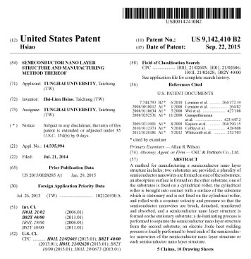
- Semiconductor Nano Layer Structure and Manufacture Method Thereof (半導體奈米層狀結構及其製作方法), 2015 USA patent No. US 9,142,410 B2, 中華民國專利申請案號102126930
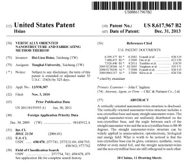
- Vertically oriented nanowires array structure and method thereof (筆直直立奈米線陣列結構及其製造方法), 2014 USA patent No. US 8,617,967 B2, 中華民國專利證書1466816
Book Chapters:
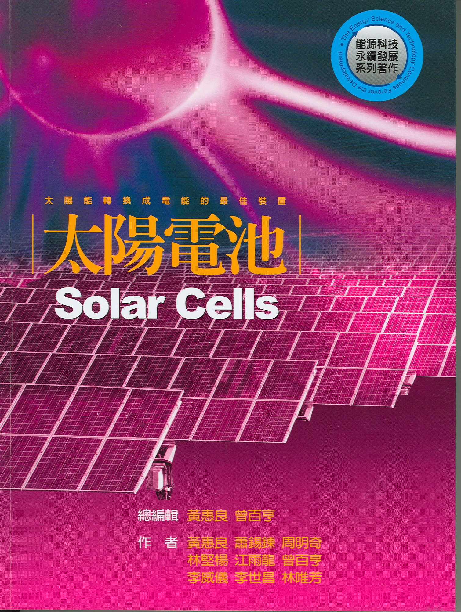
- 太陽電池 (Solar Cells), 五南叢書出版公司
- Z. Pei, H. L. Hsiao, and H. L. Hwang,“Optical and Electrical Transport Properties of Silicon Nano Dots Embedded in Siliocn-rich Nitrides”, Handbook of Semiconductor Nanostructures and Devices, 2004 American Scientific Publishers.
- Z. Pei, H. L. Hsiao, and H. L. Hwang, Advanced Luminescent Materials and Quantum Confinement, 1999
- Z. Pei, H. L. Hsiao, and H. L. Hwang, Materials Research Society Vol. 560, Luminescent Materials 1999.
- H. L. Hsiao, A.B. Yang and H.L. Hwang, Materials Research Society Vol. 507, Amorphous and Microcrystalline Silicon Technology 1998
- H. L. Hsiao, K.C. Wang, A.B. Yang, T.R. Yew and H.L. Hwang, Materials Research Society Vol. 406, Diagnostic Techniques for Semiconductor Materials Processing II 1996
Journal Papers
- S. M. Lu*, W. B. Su, C. L. Lin, W. Y. Chan, H. L. Hsiao, C. S. Chang, and Tien T. Tsong, “Disappearance of Lowest-Order Transmission Resonance in Ag Film of Critical Thickness” , Japanese Journal of Applied Physics, 50 (2011), 08LB01.
- S. M. Lu*, W. B. Su, C. L. Lin, W. Y. Chan, H. L. Hsiao, C. S. Chang, and Tien T. Tsong,
“Electron relaxation in empty quantum-well states of a Pb island on Cu(111) studied by Z-V
(distance-voltage) spectroscopy in scanning tunneling microscopy”, Journal of Applied Physics, 108
(2010)83707.
- Hsi-Lien Hsiao*, Zhan-Yuan Liu, Pin-Hui Lee, “Acetylene assisted formation of GaN–carbon nanotubes heterojunction nanowires”, Diamond and related Materials 18, (2009) 537.
- H.L. Hsiao*, A.B. Yang and H. L. Hwang, “Luminescence and Structural Properties of Silicon-rich Nitride by X-ray Absorption Spectroscopy”, Journal of Physics and Chemistry of Solid, 69 (2008) 278-283.
- L.C. Lu, Y.L. Chueh, L. J. Chen*, L.J. Chou, H.L. Hsiao, and A.B. Yang, "Synthesis and formation mechanism of gallium nitride nanotubular structure" Electrochemical and Solid State Letters 8, (2007) G153-G155.
- H.L. Hsiao*, C.Y. Chen and A.B. Yang, ”Low Temperature Selective Growth and Field Emission Characteristics of Tapered SiGe Nanowires Array”, WSEAS Transactions on Electronics 4 (2006) 179.
- M.C. Lu, Y.L. Chueh, L. J. Chen*, L.J. Chou, H.L. Hsiao, and A.B. Yang, 2005 "Synthesis and formation mechanism of gallium nitride nanotubular structure" Electrochemical and Solid State Letters 8, G153-G155.
- Z. Pei*, A.Y.K. Su, H.L. Hwang, and H.L. Hsiao, 2005 “Room temperature tunneling transport through Si nanodots in silicon rich silicon nitride”, Applied Physics Letters 86, 63503.
- H.F. Hsu, H.C. Hsu, T.F. Chiang, L.J. Chen, and H.L. Hsiao*, 2004, "Identification of the first nucleated phase in submonolayer Ti deposited on Si(111)-7x7 by atomic resolution techniques”, Ultramicroscopy 100/3-4, 347-351.
- H.F Hsu, L.J. Chen*, H.L. Hsiao, T.W. Pi, 2003: Adsorption and switching behavior of individual Ti atoms on the Si(111)-7x7 surface, Phys. Rev. B 68.
- H.L. Hsiao*, A.B. Yang and H. L. Hwang, 2003: Direct Observation of Localized Unoccupied States by Synchrotron Radiation Two-Color Resonant Photoemission”, Applied Surface Science, Volume: 212-213, May 15, pp. 73-77.
- H.F Hsu, M.C Lu, C.K. Fang, L.J. Chen*, H.L. Hsiao, T.W. Pi, 2003: Initial stages of ultra thin Ti film growth on Si(111)-7×7 surface, Thin Solid Film Volume: 428, Issue: 1-2, March 20, 2003, pp. 133-138.
Conference Papers:
- H.L. Hsiao, L.F. Chou, E. Y. Chang, Y.S. Lee, W.D. Chang, P.Y. Wang, C.Y. Tsao (2013, Nov). Tapered Silicon Nanorod Solar Cell on Aluminum Foil. 23rd International Photovoltaic Science and Engineering Conference (PVSEC-23), Taipei.
|
|
|
|
|
| |

Tel : +886-4-23590121 ext. 32141, 32150
Fax: +886-4-23594643
Contact H-L Hsiao |
Laboratoty of Advanced Materials for Photonics and Electronics (LAMPS),
P.O. Box 5-803,
Department of Applied Physics,
Tunghai University,
407 Taichung, TAIWAN
|
|
| |
|
|
|
|